

AIoT Edge Computing: From Cloud Down to the Device
Compute migrating from the cloud to the edge is reshaping IoT device architecture. This article analyzes hardware design essentials and typical scenarios for edge AI.

In 2026, edge AI is no longer a slide in a pitch deck. According to cross-referenced data from ABI Research and Counterpoint, global edge-AI chip shipments reached 4.2 billion units in 2025, up 38% year over year, while the penetration of on-device inference in industrial IoT crossed 55% for the first time. As compute migrates from the cloud to the device, it is reshaping both the hardware architecture and the software stack of IoT systems. For front-line electronics engineers, this means recalibrating every link in the chain: component selection, PCB layout, firmware, and the power budget.
Source: SIMDA project data
What Edge AI Changes in the Architecture
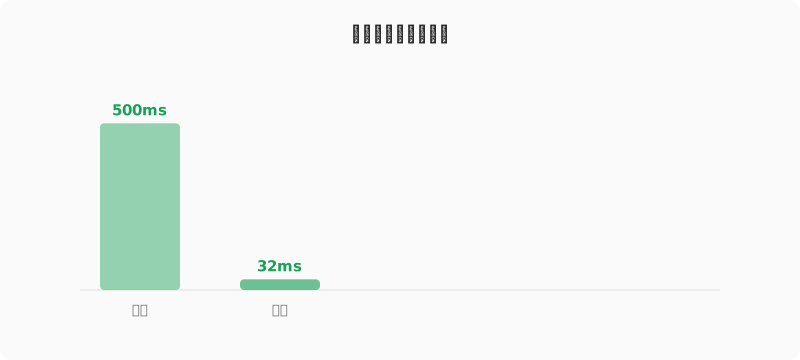
The traditional IoT architecture is a serial “sensor → gateway → cloud inference → control” chain. In industrial control, machine vision, and voice interaction, end-to-end latency on this chain typically sits between 200 and 800ms, with visible sensitivity to network jitter. Once inference is pushed to the device, end-to-end latency compresses to 15–50ms, while upstream bandwidth demand drops by one to two orders of magnitude—the cloud receives only structured results (detection JSON, anomaly alerts) rather than raw video streams or high-frequency vibration data.
Equally important are reliability and privacy. In power grids, rail, and medical applications, a network outage means an outage of the business; in face recognition and industrial inspection, keeping raw data on-device is a compliance baseline. On-device inference gives the device offline autonomy—an engineering value the cloud cannot replace. For R&D managers, it also means architecture authority is flowing back from cloud teams to embedded teams.
On the cost side, the cloud-to-edge shift reframes the total-cost-of-ownership curve. A Counterpoint TCO model for a 1000-camera industrial-vision deployment showed cloud-only inference at $0.012 per inference-hour saturating bandwidth and compute charges above $1.4M annually, while an edge-tier deployment amortized the NPU silicon into the camera BOM at roughly $11 per node, cutting annual OPEX to under $180K. The breakeven crossover lands at month 18—well within the typical 5-year industrial asset life. Latency benchmarks reinforce the case: 5G URLLC theoretical floors of 1ms are rarely sustained in production due to core-network scheduling jitter, whereas a local SoC inference path measured at 22ms end-to-end (sensor → ISP → NPU → actuator) shows standard deviation below 1.5ms. For safety-critical loops—collision avoidance, robotic collaboration—this determinism, not peak throughput, is the engineering argument that closes the deal.
Three Curves of Compute Selection
Selecting an edge-AI chip is fundamentally a balancing act across three curves: compute (TOPS), power (W), and toolchain maturity.
Tier one: low-power MCU plus lightweight NPU. Examples include ARM Cortex-M55/M85 cores paired with the Ethos-U55 NPU, or domestic RISC-V chips with in-house NPUs. Compute lands at 0.5–2 TOPS, power below 500mW—suitable for keyword spotting, gesture recognition, and single-sensor anomaly detection. Models are typically quantized TinyML workloads (INT8, parameters under 2MB) deployed via CMSIS-NN or TensorFlow Lite Micro.
Tier two: mid-range SoC with integrated NPU. Examples include Allwinner T527, Rockchip RK3588S, Amlogic A311D2, and Qualcomm QCS6490. Compute sits at 6–15 TOPS, power at 3–8W. This tier supports multi-channel MIPI-CSI camera input and composite tasks such as face recognition, object detection, and OCR—the mainstream band for current AIoT terminals with relatively mature toolchains.
Tier three: edge-server class. Examples include NVIDIA Orin Nano/NX and Huawei Ascend Atlas 200I. Compute reaches 40–100 TOPS, power 15–60W. These are deployed in roadside units (RSU), industrial-vision IPCs, and AGV central compute modules, supporting multi-precision INT8/INT16/FP16 inference and concurrent multi-model workloads on a Linux + Docker + TensorRT/CANN stack.
The most common trap engineers fall into is fixating on peak TOPS. In practice, sustained compute depends on thermal design, and effective compute depends on operator hit-rate on the NPU (typically 60%–85%). A chip rated at 8 TOPS may deliver only 40% of theoretical throughput when running YOLOv8n in the real world.
Effective throughput is best benchmarked against standardized workloads. MLPerf Tiny v2.0 results for the ResNet-50 and MobileBERT suites reveal that vendor-stated peak TOPS routinely overstate real inference-per-watt by 1.8× to 3.2×, with the gap widening for transformer-based models that exhibit poor operator locality. A more honest selection metric is inferences-per-joule at the target precision and batch size: the Cortex-M55 + Ethos-U55 pair delivers roughly 4–6 ResNet-50 inferences/J at INT8, while the Orin NX sits near 18–22 inferences/J—numbers that drop 30–45% once thermal throttling engages at sustained 50°C ambient in a fanless enclosure. We advise selection teams to require sustained-workload benchmarks (1-hour soak at 50°C ambient) under the actual deployment thermal envelope, rather than the 5-second peak runs vendors publish in their marketing decks.
Hardware-Software Co-Engineering Practice
Edge AI does not end when the model runs on a dev board. From demo to mass production, four engineering gates stand in between.
First, quantization and pruning. After INT8 quantization of an FP32 model, accuracy loss should stay within 1%–2%; latency-sensitive layers (Conv, DepthwiseConv) must be confirmed as natively supported by the NPU, or fallback to CPU execution will tank the frame rate. We recommend QAT (Quantization-Aware Training) over PTQ (Post-Training Quantization) alone.
Second, operator adaptation. Every NPU has its list of unsupported operators. Engineers consult the vendor’s operator-support table and rewrite unsupported operators equivalently—for example, decomposing a dilated convolution into two standard convolutions—or work with the vendor’s FAE to evaluate support in the next SDK release.
Third, memory and boot. The medium storing model weights directly drives cold-start time. eMMC 5.1 sequential reads run about 300MB/s; UFS 2.1 exceeds 800MB/s. For a 100MB-class model, the boot-time delta can reach 2–3 seconds, materially affecting user-perceived responsiveness. The bandwidth gap between LPDDR4X and LPDDR5 is further amplified under concurrent multi-model workloads.
Fourth, scheduling and business coupling. The NPU is a shared resource; priority scheduling across business threads, inference threads, and UI render threads must be defined jointly by firmware and algorithm teams. We have seen too many projects fall into the “great in the lab, broken in production” trap—the root cause is almost always an undefined hardware-software interface (DMA channel conflicts, interrupt priorities, memory-pool partitioning, NPU context-switch overhead) that was never frozen early in the project.
Fifth, thermal and power integrity complete the production-readiness checklist. Edge-AI SoCs exhibit steep non-linear power scaling with NPU utilization—a 2W idle rail can spike to 9W in 200µs during a YOLOv8 inference burst, demanding low-ESL decoupling (ESL < 0.3nH) and a PDN target impedance below 5mΩ at the load. Junction temperature must be held below 105°C to meet a 10-year MTBF per Arrhenius extrapolation, which in fanless enclosures drives the choice of phase-change TIM (k ≥ 3 W/m·K) and a copper heat-spreader sized to the NPU’s TDP plus a 25% safety margin. DVFS scheduling, rail sequencing per the vendor’s Power Sequencer app note, and wake-latency budgeting (LPDDR4X self-refresh exit adds 80–120µs) all enter the firmware spec. Skipping these details is the most common path from “lab demo works” to “field returns spike.”
Typical On-Device Deployment Scenarios
Across SIMDA’s project library, on-device AI is already in stable volume production:
- Face-recognition access and payment terminals: RK3566 / RK3588 designs, liveness plus 1:N matching (N ≤ 10000), end-to-end response under 400ms, total power below 5W.
- Industrial visual inspection: NVIDIA Orin NX, YOLOv8s plus a defect-classification second stage, line beat 60 PPM, missed-defect rate under 0.3%.
- AGV/AMR navigation: multi-sensor fusion plus VSLAM, on-device path planning under 30ms, autonomous obstacle avoidance without the cloud, motion commands issued over CAN.
- Predictive maintenance: Cortex-M4 plus TinyML, vibration-spectrum anomaly detection, power below 100mW, three-year life on a single lithium cell.
Two cross-cutting lessons emerge from these deployments. First, the data pipeline—not the model—tends to dominate operations cost once in volume: an industrial-vision line generating 2 TB/day of raw frames demands an on-device retention policy (typically anomaly-only capture, ≤ 5% of frames) and an OTA-trained model refresh path. Second, MLOps for edge devices differs materially from cloud MLOps: device-side models must ship with rollback partitions, A/B inference selection, and a telemetry schema that surfaces inference-latency percentiles (P50/P95/P99) and NPU utilization—not just accuracy. On one predictive-maintenance rollout, monitoring P99 latency exposed a thermal-throttle event the accuracy metric had masked for three weeks, allowing a TIM retrofit before field failure. Edge MLOps is, fundamentally, an embedded-systems discipline with a model dimension—not a cloud discipline ported to silicon.
Conclusion and Recommendations
Over the next decade of edge AI, compute will keep moving down, but what moves down with it is responsibility. Once decisions migrate from cloud to device, engineers own latency, power, reliability, and security end to end.
We offer three recommendations. First, work backward from production metrics during selection—frame rate, boot time, thermal rise, long-term MTBF—rather than letting demo frame rate drive the decision. Second, establish a joint review across model, firmware, and hardware teams, with interface freeze (DMA, interrupts, memory pools, NPU scheduling) entered as a project milestone. Third, reserve an OTA model-update channel—on-device models iterate on a cycle far longer than the hardware, and OTA is the only sustainable evolution path.
Fourth, and easily underestimated: plan for end-of-life at the SoC level. Edge-AI silicon moves on an 18-month cadence; the SoC qualified today will likely be NRD (Not Recommended for Design) within 36 months. Lock the firmware abstraction against the SoC vendor’s BSP, document the kernel and toolchain pinning, and negotiate a last-time-buy commitment aligned to the product’s service horizon. We have seen clients stranded on a single Korean SoC whose vendor exited the segment mid-product-life, forcing a 14-month port to an alternative platform at ten times the original NRE. Treating the SoC as a lifecycle-managed asset, not a commodity, is one of the highest-leverage decisions in edge-AI engineering.
SIMDA has sedimented end-to-end on-device AI engineering experience across edge-computing main boards, face-recognition terminals, AGV robots, and industrial-vision projects, covering the full ARM Cortex-A/M family, RISC-V, NVIDIA Jetson, and domestic NPU platforms. From component selection and schematic design through firmware development, model deployment, and mass production, we make models run stably on real products.