

DFM: Lifting Mass-Production Yield from 85% to 98%
A working prototype does not guarantee producible volume. DFM is the bridge between design and manufacturing, and it sets the ceiling for mass-production yield.

A prototype that passes EVT is not a license to mass-produce. The cruelest case we have seen: a 91% yield at EVT collapsed to 76% in the first week of mass production (MP), with single-board rework cost consuming the entire batch margin. Postmortem analysis showed that 90% of the defects traced back to DFM (Design for Manufacturing) gaps in design: BGA escape routing beyond the fabricator’s process window, V-Cut stress cracking 0201 capacitors, and test points that missed critical power rails. A one-week DFM review during design would have saved a month of firefighting at ten times the cost on the production line.
DFM is not a department or a single step—it is a methodology that runs through schematic, layout, mechanical, pilot run, and mass production. Its essence is to push factory process capability, test equipment accessibility, and component purchasability upstream into design constraints. Below we unpack the three dimensions—DFM, DFT, DFC—against IPC standards and real production data.
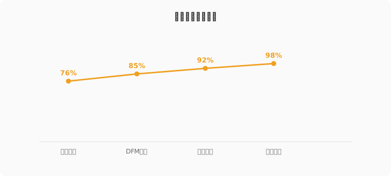
Source: SIMDA project data
1. DFM: Process Boundaries from Trace to Panel
Problem. The most common CAM rework order is “trace width/space exceeds process capability.” BGA fanout areas are especially hard hit. For a 0.4mm-pitch BGA the escape channel allows only 0.075mm / 0.075mm, yet many designers copy the 0.1mm / 0.1mm used in prototypes. At volume the etch factor erodes 20% of trace width, impedance drifts 8Ω, and differential pairs de-couple.
Root Cause. The root cause is information asymmetry between design and fabrication. Designers do not know the fabricator’s true Process Capability, and the CAM engineer often raises the alarm 24 hours before launch—far too late to respin. IPC-2221 provides recommended widths, but for volume you must derate by 15-20% against the fabricator’s stated capability.
Design Parameters. Production-ready geometry based on IPC-2221 and multiple tier-1 fabricators:
- BGA-area minimum trace / space: 0.075mm / 0.075mm (for 0.4mm-pitch BGA)
- Non-BGA default trace / space: 0.12mm / 0.12mm
- Minimum via drill: 0.20mm with 0.40mm pad
- Impedance tolerance: single-ended ±7%, differential ±10% (e.g., 100Ω ±10Ω)
- Outer-layer copper: 1oz (35μm); for dense routing use 0.5oz to reduce side etch
- Width-to-thickness per IPC-4562; never run 0.075mm traces on 2oz copper
Verification. Run a DFM audit (CAM350, Valor NPI) post-layout, focusing on: BGA channel utilization below 85%, 3D impedance simulation coupling width, copper thickness and dielectric constant, solder-mask web ≥ 0.08mm. We require an independent DFM engineer sign-off before any production release, which dropped CAM rework from 12% to 1.5%.
A frequently-overlooked second-order issue is copper distribution balance. IPC-2221 calls for ≤ 70% and ≥ 30% copper density per layer to prevent press warp; in practice, dense BGA fields push outer-layer copper above 85% locally while sparse signal areas sit below 20%, producing 1.5–2.0mm warp on a nominally flat 1.6mm board and BGA solder opens at reflow. The remedy is copper thieving (non-functional fills) on outer layers and a global copper-balance target of 60–65%. Pair this with the fabricator’s stackup-deviation report (Dk ±0.1, dielectric thickness ±10% per IPC-4101) before signing off on impedance-sensitive layers—these tolerances convert a paper 100Ω ±10Ω design into 100Ω ±14Ω in glass, which is enough to close a 25G eye. Reviewing copper balance at layout sign-off, not at CAM hand-off, is the cheap window to fix a problem that becomes very expensive after lamination.
2. Panelization and V-Cut: The Underestimated Stress Trap
Problem. A typical failure: 30mm × 40mm single board, 5 × 5 panel, V-Cut down the center. After depaneling the 0201 capacitor crack rate hit 2.3% because the V-Cut remaining web thickness was too thin, transmitting bending stress through the PCB into the component solder joints.
Root Cause. V-Cut remaining web thickness (about one-third of board thickness, ≈ 0.33mm for a 1.0mm board) is the critical parameter. Too thin and depaneling stress warps the whole board; too thick and depaneling is difficult. IPC-2221 specifies V-Cut depth tolerance ±0.05mm, but most designs never constrain the minimum distance from components to the V-Cut line.
Design Parameters:
- V-Cut remaining web: 30-40% of board thickness (0.30-0.40mm for a 1.0mm board)
- Minimum component-to-V-Cut distance: 0.4mm (small R/C) to 5.0mm (aluminum electrolytic, BGA)
- Crack-prone parts (0201, crystals, ceramic caps) forbidden on the V-Cut line; keep them ≥ 3.0mm away
- For high-stress zones use mouse-bite breakaways: 0.5mm holes, 0.8mm spacing, 5 holes per tab
- Process edge ≥ 5.0mm for SMT clamping and AOI
Verification. Run depaneling stress simulation, or physical depanel cross-section plus drop testing. During pilot run, sample 50 boards for micro-sectioning; track crack rate against a target below 0.3%.
A second stress vector is conformal coating and potting interaction. V-Cut lines that pass within 5mm of conformal-coated regions can wick coating into the score line during application, then crack the coating as the board flexes in thermal cycling (−25 to +65°C per IEC 60068-2-1/2). For coated assemblies we recommend a 6–8mm keep-out from any V-Cut, paired with a 0.3mm relief slot at score terminations. On drop-tested assemblies (1.5m drop per IEC 60068-2-31), the failure mode shifts to component-level: 0201 capacitors near the V-Cut show solder-joint fatigue an order of magnitude faster than mid-board parts. Plan the panelization with the coating and drop-spec in hand, not after the fact—retrofitting a keep-out zone after pilot build usually means a board respin.
3. DFT: Test-Point Coverage Determines Defect Interception
Problem. One project had only 62% in-circuit test (ICT) coverage with flying probe. FCT yield was 96%, but 3.8% of boards failed after 72 hours of burn-in at the customer. Root cause: no test points on key power rails (DC-DC outputs, PLL supply), so ICT could not catch regulator output deviation.
Root Cause. The core DFT (Design for Test) tension is between test-point count and PCB area / signal integrity. You cannot sprinkle test points on high-speed signals (they add parasitic capacitance), but power, reset, and clock-enable nodes must have them.
Design Parameters:
- ICT test-point coverage ≥ 90% by node count; critical nodes 100%
- Test-point diameter ≥ 0.9mm, spacing ≥ 1.8mm (bed-of-nails compatible)
- No test points under BGAs or connectors within 0.5mm
- High-speed differential test points via 0.1pF probe pads, located within 5mm of the receiver
- Boundary-scan (JTAG) coverage ≥ 80%; TCK ≤ 10MHz with 50Ω matched test points
Verification. Generate a DFT coverage report (GenRad / Agilent 3070). During pilot, run 100% flying-probe testing and record First Pass Yield per test point to locate design blind spots.
A subtler DFT tension is test-point access versus signal integrity. Test points on 10Gbps+ signals act as capacitive stubs; even a 0.1pF probe pad shifts the impedance by 3–4Ω and adds a measurable reflection. The production-grade approach is to designate “test-only” nodes (power rails, reset, slow control buses) at 100% coverage, while high-speed signals rely on boundary-scan (JTAG) and built-in self-test (BIST). For DDR4 and PCIe designs we typically reach 85–90% structural coverage through ICT plus JTAG, then close the remaining gap with functional-test fixtures. Document the test strategy in a Test Coverage Matrix at the start of layout, not at the end—retrofitting test points into a finished layout is the slowest path to a production release and almost always compromises SI.
4. DFC / Component Layout: From Nozzle to Assembly Tolerance
Problem. A tall component (an 11mm electrolytic) placed beside a BGA caused pick-and-place nozzle interference; post-reflow the BGA had a 4.1% open-solder rate. In another case, an odd-form connector 2mm from the board edge was hit by the clamping jaw and scrapped.
Root Cause. DFC (Design for Component / Assembly) failures stem from layout engineers not knowing the physical constraints of the placement machine: nozzle geometry, placement sequence, jaw travel. None of this is in the component datasheet; it must be pulled back from the factory process team.
Design Parameters:
- Tall parts (above 6mm) keep ≥ 5.0mm from BGA edges
- Odd-form parts and connectors ≥ 3.0mm from board edge to avoid jaw collision
- Same-type parts oriented uniformly for AOI and placement-path optimization
- Polarized parts (diodes, tantalum caps) need clear polarity markings ≥ 0.5mm from pads
- Wave-solder-side parts ≥ 1.27mm apart (wave fixture compatible)
- Heavy parts (above 30g) require adhesive anchor silkscreen at four corners
Verification. Run virtual placement with Siemens Valor Process Preparation to check nozzle-component-neighbor interference. Perform First Article Inspection; target placement DPMO below 500.
A second-order constraint is moisture sensitivity level (MSL) management. Per IPC/JEDEC J-STD-020, large BGAs and QFNs typically ship at MSL 3 or 4, meaning a floor life of 168 hours (MSL 3) or 72 hours (MSL 4) before they absorb enough moisture to popcorning-damage during reflow. Layout and procurement must coordinate: parts with shorter floor life should sit on early-placement lanes and use vacuum-sealed dry-pack logistics, with the floor-life clock started at the SMT line rather than at the warehouse. On one automotive project, mismatched MSL handling caused 1.4% popcorning failures that surfaced only after thermal-cycle stress testing, three weeks into a pilot build. Build MSL tracking into the pick-and-place program and warehouse issuance discipline from day one—it is far cheaper than chasing a hidden failure mode through three weeks of cross-sectioning.
The Data Loop: From Pilot to Mass Production
The true value of DFM is the data loop: pilot-run defect distribution (by type, location, batch) feeds back into design and is iterated into the next revision. We have codified this across 200+ PCB deliveries, lifting client mass-production yield from an average of 85% to over 98%. The practice:
- Run ≥ 100 boards through pilot; record defect type, coordinates, and rework action per board
- Pareto-rank defects; the TOP3 must be fixed in the current revision, not deferred
- Maintain a DFM rule library, each rule tied to an IPC clause, factory data, and a failure case
- Cross-functional sign-off: hardware, layout, process, test, procurement
The data loop also has a regulatory dimension for medical and automotive projects. IPC-A-610 Class 3 (high-performance electronic products) and IEC 62304 (medical device software lifecycle) both require documented process-capability evidence; a well-kept DFM rule library doubles as that evidence. Each rule, tied to an IPC clause and a defect-prevention case, can be exported as part of the device master record—turning what was once engineering folklore into auditable quality documentation. For clients pursuing FDA 510(k) submissions or automotive PPAP packages, this conformance traceability is often the difference between a clean review and a multi-round deficiency response.
DFM is not a cost—it is an investment. A design done right the first time saves the entire line from rework, recall, and brand damage. Lifting yield from 85% to 98% is, fundamentally, trading a little design diligence for a lot of production peace of mind.