

5 Key Principles of High-Speed PCB Signal Routing
Once signal rates break past 10 Gbps, routing is no longer "just connect it." This article summarizes the core principles and common pitfalls of high-speed PCB layout.

Once signal rates enter the Gbps range, PCB traces stop being “electrical connections” and become “transmission lines.” Every inch of trace is a trade-off among impedance, loss, and crosstalk. We recently built a 25G SerDes board where the engineering prototype was routed with a “just connect it” mindset—the link pinged fine, but the eye-mask margin went negative and BER collapsed at 1E-6. The postmortem showed the problem was not the chip but the layout’s disregard for transmission-line physics. High-speed design has no silver bullet, but the five principles below—hard constraints refined over 80+ high-speed board deliveries—will keep you out of most traps.
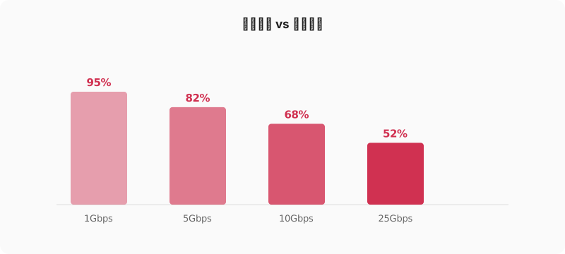
Source: SIMDA project data
1. Impedance Continuity Matters More Than Exact Impedance
Problem. Engineers often agonize over 50Ω versus 90Ω differential, but the real killer is impedance discontinuity. The three common discontinuities are via stubs, reference-layer changes, and connector transition regions. A 25G signal on a 0.25mm via stub can see -8dB return loss—the eye closes outright.
Root Cause. A signal propagates as an electromagnetic wave; any impedance step reflects. A via stub acts as an open-circuit stub that resonates at specific frequencies; a reference-layer change severs the return path and causes an impedance jump. IPC-2141A gives impedance formulas, but measured deviation requires TDR (Time-Domain Reflectometry).
Design Parameters:
- Single-ended impedance: 50Ω ±7% (use IPC-2141A to size trace width)
- Differential impedance: 100Ω ±10% (USB3.0, PCIe, SerDes standard)
- Impedance control mandatory when trace length exceeds Tr/6 (Tr = rise time)
- Via stub length ≤ 10mil (0.25mm); otherwise use back-drilling
- High-speed layers need a solid reference plane; never route across split power planes
- Width sized for impedance (typical FR-4, Dk 4.0, 0.1mm dielectric, 0.18mm width → 50Ω)
Verification. Run full-path impedance simulation (HyperLynx / Ansys SIwave) post-layout; output a TDR impedance curve with target variation ≤ ±10%. After fabrication, sample-test ≥ 5 boards with a real TDR.
A second-order discontinuity that escapes rule-checks is the connector-to-board transition. A high-speed connector (SFP+, QSFP, MCX) introduces a 4–8mm region where the signal leaves the controlled-impedance PCB and traverses contact fingers, plated through-holes, and the connector’s internal geometry—typically a 10–15Ω step that creates reflections of −15 to −20dB at 25Gbps. The fix is co-design with the connector vendor’s 3D model (HFSS / CST), tuning the launch-pad geometry and the partial-via back-drill depth to flatten the impedance profile through the transition. On one 100G Ethernet design this co-design raised eye-mask margin from a marginal 8% to a comfortable 28%, with no board respin—just a launch-pad shape revision caught in the pre-fabrication review.
2. Differential Pairs: Spacing Before Length Matching
Problem. Engineers habitually length-match first and adjust spacing second, breaking differential coupling. In one PCIe Gen3 project, length matching stretched the coupling gap from 0.15mm to 0.3mm; the differential-to-common-mode conversion (SCD21) degraded from -30dB to -18dB, and EMC radiation exceeded the limit by 6dB.
Root Cause. A differential pair’s common-mode noise rejection depends on tight coupling between the two traces. Wider spacing weakens coupling, increases noise sensitivity, and shifts energy from differential to common mode. Length matching is for timing, but blind length matching (accordion, sawtooth) sacrifices coupling.
Design Parameters:
- Differential coupling gap: 0.15-0.20mm (for 0.12mm trace width)
- Differential length mismatch ≤ 5mil (0.127mm) at 10Gbps; ≤ 2mil at 25Gbps
- Length compensation preferably near the receiver (within 5mm), using symmetric tuning
- Spacing between adjacent differential pairs ≥ 3× trace width (the 3W rule) to cut far-end crosstalk
- Never change layers within a differential pair; if unavoidable, keep the two vias ≤ 0.5mm apart with a ground-via escort
Verification. Extract the differential S-parameters (SDD11, SDD21, SCD21). Require SDD21 ≥ -3dB at Nyquist and SCD21 ≤ -25dB. Verify mixed-mode S-parameters on a 4-port VNA.
An adjacent issue is skew from fiberglass weave. FR-4 is a woven composite; traces that run along a yarn bundle see Dk ≈ 4.4, while traces between bundles see Dk ≈ 3.9—a 0.5 Dk delta that introduces 2–4ps of intra-pair skew per inch at 25Gbps, well above the 1ps budget for a tightly coupled SerDes link. Mitigations include “zig-zag” routing at 5–10° off-axis (per IPC-2141A guidance), specifying low-Dk-spread laminates (Megtron 6, Tachyon 100G) for ≥ 25Gbps links, and rotating the panel artwork 10–15° relative to the laminate weave. Pre-layout simulation alone misses this effect because the stackup model assumes a homogeneous Dk; only fabrication-with-measurement on a characterized weave spread closes the analysis and explains why two “identical” boards from different fabricators can show divergent eye margins.
3. Power Integrity Is the Foundation of Signal Integrity
Problem. In a DDR4 project, the SI was dialed in but the power-rail ripple hit 80mVpp, triggering spurious logic flips in the core. Only one decoupling value (0.1μF) was used; the PDN impedance at the target decoupling frequency (100MHz) was 0.8Ω—far above the 0.1Ω target.
Root Cause. The return path of high-speed signals depends on a solid ground plane and a low-impedance Power Distribution Network (PDN). Decoupling capacitor type, value, and mounting inductance (ESL) determine the PDN impedance in the target band. A single capacitor value turns inductive above its self-resonant frequency and loses decoupling effect. IPC-2152 current-capacity curves feed directly into PDN design.
Design Parameters:
- Target PDN impedance Ztarget = (Vcc × ripple%) / ΔI; e.g., 1.2V ±3% / 5A → 7.2mΩ
- Decoupling mix: 10μF (tantalum) + 1μF (ceramic) + 0.1μF (ceramic) + 0.01μF (ceramic)
- Critical: capacitor ESL < 0.5nH, mounting loop inductance < 0.5nH
- Layout: smaller values closer to the chip’s power pins; 0.01μF within 3mm
- Power plane adjacent to ground plane, dielectric ≤ 0.1mm, to maximize plane capacitance
- Shorting-via density ≥ 1 per 5mm² to shorten the return path
Verification. Run a full-board PDN simulation (Ansys SIwave) to produce Z(f); require Z ≤ Ztarget across 1kHz-1GHz. Verify on hardware with a VNA measuring the rail’s self-impedance.
A common PI oversight is decoupling-capacitor anti-resonance. Each capacitor’s impedance curve has a minimum at its self-resonant frequency and rises inductively above it; when multiple values are paralleled, their inductive branches interact with the plane-pair capacitance to produce anti-resonance peaks—often 2–5× higher than Ztarget in the 100–500MHz band. The remedy is a deliberate mix of package sizes (0402 for high-frequency, 0603 for mid-band, 0805 for bulk), each chosen for its ESL rather than its capacitance alone, and verified by full-board PDN simulation including the plane pair. A useful rule of thumb: target ≤ 3 decoupling capacitors per power pin in the high-frequency path, with ESLs staggered at roughly 0.3nH / 0.6nH / 1.2nH to spread the resonance peaks rather than piling them at a single frequency.
4. Crosstalk Isolation Starts at Placement
Problem. On a mixed-signal board, the ADC clock line ran parallel to FPGA LVDS for 30mm at 0.2mm spacing. Clock jitter hit 12ps and ADC SNR dropped 4dB—caused by far-end crosstalk (FEXT) from the LVDS pair.
Root Cause. Crosstalk is the mutual capacitance (Cm) and mutual inductance (Lm) coupling between adjacent traces. Coupling scales with parallel length, inverse spacing, and signal edge rate. The 3W rule (spacing ≥ 3× width) keeps crosstalk below -50dB; if you do not reserve isolation space at placement, layout cannot recover it.
Design Parameters:
- High-speed adjacent spacing ≥ 3W (W = trace width); critical signals ≥ 5W
- High-speed to analog spacing ≥ 5W with a grounded guard trace between
- Sensitive signals (clock, reset) ≥ 5mm from switching regulators, inductors, crystals
- Long parallel runs (length greater than signal rise length) must route as stripline on inner layers
- Ground-via escort: one ground via every 1/10 wavelength alongside high-speed pairs
- Crosstalk limits: NEXT ≤ -50dB, FEXT ≤ -40dB
Verification. Post-layout crosstalk simulation (HyperLynx) producing NEXT / FEXT vs frequency. Run a routing audit script (Allegro DFI) to flag parallel segments that are too long or too close.
Crosstalk analysis should also cover the power/ground via field. A high-speed signal via that traverses multiple plane pairs creates a discontinuity in the return path; without adjacent ground vias to escort the return current, the signal energizes the plane cavity and radiates as a system-wide noise source. The convention is to place a ground via within 1.5× the anti-pad distance of every high-speed signal via, and to ensure the cavity between reference planes is below λ/20 at the highest frequency of interest (e.g., < 1.5mm at 25GHz on FR-4). Post-layout EM extraction (HFSS, Clarity) catches cavity resonances that 2D field solvers miss entirely—these are the silent killers of multi-link SerDes designs where one noisy link contaminates every neighbor on the same layer.
5. Simulation Is Verification, Not Design
Problem. The classic anti-pattern: route first, simulate later. After layout the SI simulation reveals discontinuities and crosstalk violations, but the board is already in fabrication—changes are expensive. Simulation degrades into a post-mortem.
Root Cause. Simulation’s real value is to drive constraints (width, spacing, stackup, placement) early. If you route before simulating, the tool can only tell you what’s wrong, not fix it cheaply. The right order: simulate to build constraints, route within constraints, simulate last for final confirmation.
Design Parameters:
- Stackup design: simulate each layer’s impedance, dielectric thickness, copper thickness, and reference-layer integrity
- Pre-layout simulation: topology, length, and termination (e.g., DDR4 ODT 40Ω) for critical signals
- Constraint-driven routing (Constraint Manager): width, spacing, length tolerance, differential rules
- Post-layout simulation: full-path SI, crosstalk, and joint SI-PI
- Models: vendor IBIS / IBIS-AMI models valid up to Nyquist (25Gbps → 12.5GHz)
Verification. Simulation should output eye-mask margin (≥ 20%), jitter budget (RJ + DJ ≤ 15% UI), and SSO noise. After fabrication, measure the eye with a high-speed scope; require correlation R² ≥ 0.9 against simulation.
A discipline worth adopting is simulation-test correlation as a closed loop. After fabrication, capture TDR, VNA S-parameters, and eye diagrams on the actual board, then back-correlate to the pre-layout simulation (R² ≥ 0.9 on impedance profiles and insertion-loss curves). Deltas below R² = 0.9 indicate the simulation model is missing something—often a stackup tolerance, a connector transition, or a weave effect—and the next project’s setup should be updated accordingly. Over our last 30 high-speed board deliveries this correlation discipline has compressed pre-silicon validation time by roughly 40%, because the simulation became trustworthy enough to release to fabrication without a physical contingency respin.
Conclusion
High-speed design is systems engineering, and the five principles are coupled: impedance continuity depends on stackup, differential coupling depends on spacing rules, PI on capacitor placement, crosstalk on isolation space, and simulation on upfront constraints. There is no silver bullet, but following these five hard constraints will keep you out of 80% of common traps. The remaining 20% is covered by experience and pilot-run data, and disciplined simulation-to-test correlation can lift that trap-free figure above 95% on subsequent revisions.